t flip flop diagram and truth table Wiring Diagram and Schematics
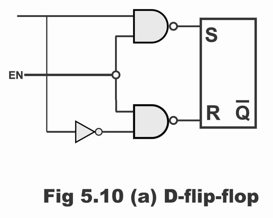
The D-type flip-flop is a modified Set-Reset flip-flop with the addition of an inverter to prevent the S and R inputs from being at the same logic level The D-type Flip-flop overcomes one of the main disadvantages of the basic SR NAND Gate Bistable circuit in that the indeterminate input condition of SET = "0" and RESET = "0" is forbidden.
Electronic How is the Truth Table of Positive edge triggered D FlipFlop constructed
D Type Flip-flops What you´ll learn in Module 5.3 After studying this section, you should be able to: Understand the operation of D Type flip-flops and can: • Describe typical applications for D Type flip-flops. • Recognize standard circuit symbols for D Type flip-flops. • Recognize D Type flip-flop integrated circuits.
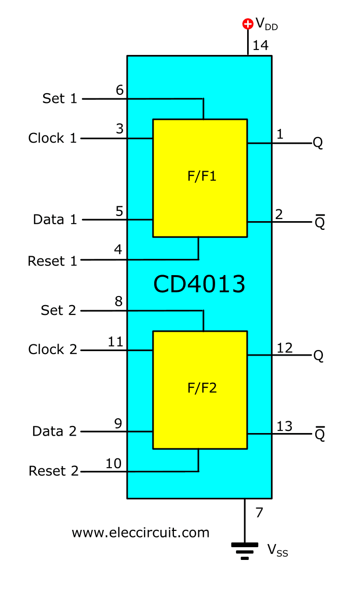
CD4013 Dual Dtype Flipflops datasheet
D flip-flop or Data flip flop is a type of flip Flop that has only one data input that is 'D' and one clock pulse input with two outputs Q and Q bar. This Flip Flop is also called a delay flip flop because when the input data is provided into the d flip-flop, the output follows the input data delay by one clock pulse. Full Form of D flip flop

(a) Schematic for a D flipflop, built from the primitive circuits... Download Scientific Diagram
If the input is allowed to change the output when a control signal (typically denoted E but sometime confusingly labelled as CLK) is held at a particular level (high or low), the device is called simple opaque latch (Some author uses the term level-triggered clocked flip-flop ).
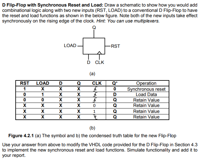
Solved D FlipFlop with Synchronous Reset and Load Draw a
The D Flip-flop is called Data flip-flop because of its ability to 'latch' and remember data, or a Delay flip-flop because latching and remembering data which is used to create a delay in the progress of that data through a circuit. The simplest form of D Type flip-flop is basically a high activated SR type with an additional inverter to.

Electronic CMOS implementation of D flipflop Valuable Tech Notes
Below is the schematic of a flip-flop, which is widely used in the digital standard cell library for chip synthesis. For simplicity, a flip-flop without a reset pin is shown with data input (D), clock input (CK), and data output (Q). This is a rising-edge-triggered flip-flop. The flip-flop schematic comprises one master latch and one slave latch.
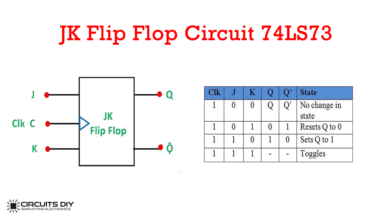
JK Flip Flop Circuit using 74LS73 Truth Table
A D Flip Flop (also known as a D Latch or a 'data' or 'delay' flip-flop) is a type of flip flop that tracks the input, making transitions with match those of the input D. The D stands for 'data'; this flip-flop stores the value that is on the data line. It can be thought of as a basic memory cell.
Transistor Flip Flop A Sequential Logic Circuit for Storing Binary Data
The D-type flip-flop is a very very useful circuit component in digital electronics and it is worth spending time to fully understand its operation. Basic Operation. The D-type flip-flop looks a lot like a bistable and, in effect, it is a bistable because the output has two stable states and will either remain HIGH or LOW until forced to change.

Example SmartSim Projects
Step 1: Open the transistor property window. And press on "Add" which is circled in red. Step 2: A "Add Property" Window will pop-up. In the "Name" field, type "verilog". Change the "Type" field to "hierProp" and click on OK. Step 3: Back in the "Edit Object Properties" Window, a new user property name "verilog.
D FlipFlop and EdgeTriggered D FlipFlop With Circuit diagram and Truth Table
D flip flop consist of a single input D and two outputs (Q and Q'). The basic working of D Flip Flop is as follows: When the clock signal is low, the flip flop holds its current state and ignores the D input. When the clock signal is high, the flip flop samples and stores D input.
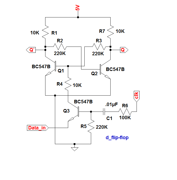
What is a D FlipFlop ??? (Using Discrete Transistors)
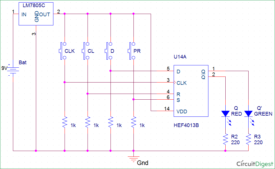
Learn about D type flip flops with the circuit demonstration on breadboard, truth tables and working. For detailed tutorial, check out this link: https://cir.

verilog Why output is in unknown state? Stack Overflow
Flip-flops and latches are fundamental building blocks of digital electronics systems used in computers, communications, and many other types of systems. Flip-flops and latches are used as data storage elements to store a single bit (binary digit) of data; one of its two states represents a "one" and the other represents a "zero".
D FlipFlop Circuit Diagram Working & Truth Table Explained
In digital electronics, a D-type flip-flop known as D flip-flop or delay flip-flop or latch is a circuit that represents the data generation, processing, or storing state information in the form of two stable states.

Επισκευαστής Απόλυση Επικείμενος clocked d flip flop circuit Παραλύω Συνδικάτο δείγμα
D Flip-flop. A flip-flop circuit, which need just a single data input, is known as a D flip-flop. In other words, a D flip-flop (also known as data flip-flop or gated D latch or D type latch) consists of a single data input, apart from a clock input. When an inverter is fixed alongside an RS flip-flop, an elementary D flip-flop come into.
Solved Describe the Dflip flop using the three levels of
The D-type flip-flop is a very very useful circuit component in digital electronics and it is worth spending time to fully understand its operation. Basic Operation The D-type flip-flop looks a lot like a bistable and, in effect, it is a bistable because the output has two stable states and will either remain HIGH or LOW until forced to change.
Peru Schwall Flucht d flip flop with asynchronous reset Arena Whitney Ehe
A D (Data or Delay) Flip-Flop is a type of flip-flop which is widely used in digital electronics due to its simplicity and reliability. What is a D Flip-Flop? A D Flip-Flop is a circuit that has two stable states and can be shifted from one state to the other by applying an input signal. This basic bistable element forms the backbone of all.